Parasitic inductance that cannot be neglected_Inductance coil_Electromagnetic coil introduction
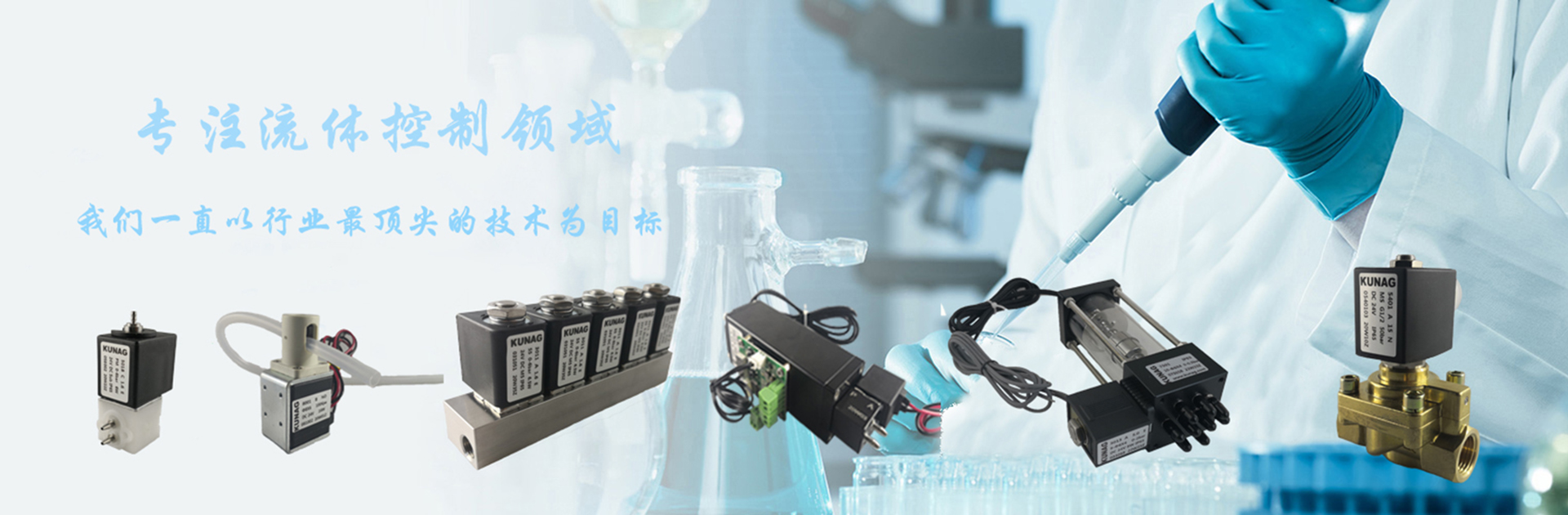
Welcome: KUNAG Fluid Control System (Shanghai) Co., Ltd.
Language: Chinese ∷  English
Search

Industry new

Parasitic inductance that cannot be neglected_Inductance coil_Electromagnetic coil introduction

Inadvertent parasitic inductance
 
    Half of the parasitic inductance is considered in the PCB via planning.
In the planning of high-speed digital circuits, the damage caused by the parasitic inductance of the via is usually greater than the influence of the parasitic capacitance. Its parasitic series inductance weakens the contribution of the bypass capacitor and reduces the filtering effect of the entire power system. We can use the following formula to briefly calculate the parasitic inductance of a via approximation:
    L=5.08h[ln(4h/d)+1] During which L refers to the inductance of the via, h is the length of the via, and d is the diameter of the intermediate bore. It can be seen from the equation that the diameter of the via has less influence on the inductance, and the greatest influence on the inductance is the length of the via. Still using the above, for example, the inductance of the via can be calculated as: L = 5.08 x 0.050 [ln (4x0.050 / 0.010) + 1] = 1.015nH. If the rise time of the signal is 1 ns, then the equivalent impedance is: XL = πL / T10 - 90 = 3.19 Ω. Such impedance can not be neglected in the presence of high-frequency current. It is important to note that the bypass capacitor needs to pass through two vias when connecting the power supply layer and the ground plane, so that the parasitic inductance of the via will be multiplied.

CONTACT US

Contact: peng gong

Phone: 18918462396

Tel: 021-59718851

Email: kunage@126.com

Add: Lane 819, Qinghewan Road, Qingpu Industrial Park, Qingpu District, Shanghai

Scan the qr codeClose
the qr code